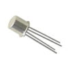
This device is designed for low level analog switching, sample and hold circuits and chopper stabilized amplifiers. It’s Source & Drain are interchangeable.
Features:-
- Low Error Voltage
- High-Speed Analog Circuit Performance
- Negligible “Off-Error,” Excellent Accuracy
- Good Frequency Response, Low Glitches
- Eliminates Additional Buffering
Detailed Specifications:-
| Transistor Polarity | N-Channel |
| Gate-Source Voltage (VGSS) | 35V |
| Drain-Source Current (IDSS) | 50mA |
| Drain-Source Resistance (Rds On) | 50Ohms |
| Input Capacitance (Ciss) | 2pF |
| Gate to Source Forward Voltage (VGS(F)) | 0.7V |
| Gate to Source Cutoff Voltage (VGS(OFF)) | 5V |
| Reverse Transfer Capacitance (Crss) | 5pF |
| Operating Temperature Range | -55 – 125°C |
| Power Dissipation (PD) | 625mW |


![j112-jfet-transistor-400x400[1]](https://cherryelectronics.in/wp-content/uploads/2023/11/j112-jfet-transistor-400x4001-1.jpg)
![j112-jfet-transistor-400×400[1]](https://cherryelectronics.in/wp-content/uploads/2023/11/j112-jfet-transistor-400x4001-1-100x100.jpg)


Reviews
There are no reviews yet.