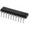

The 74LS280 IC designed as a Universal 9-Bit Parity Generator /Checker. These IC provides odd/ even outputs to facilitate either odd or even parity. By cascading, the word length is easily expanded. The 74LS280 IC operates at a wide range of working voltage, a wide range of working conditions. And directly interfaces with CMOS, NMOS, and TTL. The output of the IC always comes in TTL which makes it quite easy to function with other TTL devices and microcontrollers. The IC 74LS280 comes as smaller in size and offers much faster speed which makes it highly reliable in every kind of device.
The 74LS280 was designed without the expander input implementation, but the corresponding function provided by an input at Pin 4 and the absence of any connection at Pin 3. This design permits the IC to substituted for the LS180 which results in improved performance. It also consists of buffered inputs to lower the drive requirements to one LS unit load.
A parity generator designed as a combinational logic circuit that generates the parity bit in the transmitter. In short, it is a circuit that checks the parity in the receiver known as a parity checker. A combined circuit or devices of parity generators and parity checkers widely used in digital systems to detect the single-bit errors in the transmitted data word. Hence the sum of the data bits and parity bits can be even or odd. In even parity, the added parity bit will make the total number of 1s an even amount. Whereas in odd parity the added parity bit makes the total number of 1s odd amount
Applications :-
- Used to detect errors in transmitted data caused by noise or other disturbances.
Specifications :-
- 9 Bit Odd or Even Parity Generator or Checker
- Supply Voltage Range: 4.75V to 5.25V
- Supply Current Max : 27mA
- HIGH Level Input Voltage Min.: 2V
- LOW Level Input Voltage Max.: 0.8V
- HIGH Level Output Voltage Min.: 2.7V
- LOW Level Output Voltage Max.: 0.5V
- High level Output Current Max.: -0.4mA
- Low level Output Current Max.: 8mA
- Input Clamp Voltage Max.: -1.5V
- Propagation Delay Time Max.: 50ns
- Typical Power Dissipation: 80mW
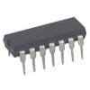
- Package: DIP-14
Package Includes :-
1 X 74LS280 9-Bit Odd-Even Parity Generator Checker IC (74280) DIP-14 Package


Reviews
There are no reviews yet.